Contents of the invention
The purpose of the application is to provide a design method for metasurface parts and related equipment and optical system optimization methods, so that the designed metasurface parts can realize the functions jointly realized by the combination of replaced optical components, so as to facilitate the simplification of the structure of the optical system.
first, the application provides a metasurface piece design method for designing a metasurface piece for replacing the target module in the optical system, the optical system comprises a light source, an optical sensor and at least one optical element arranged between the light source and the optical sensor, wherein at least one continuous optical element constitutes the target module, all devices on the front side of the target module form a forward module, and all devices on the rear side of the target module form a backward module;
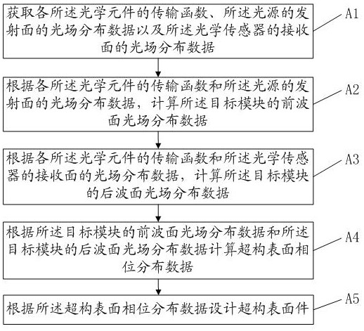
The metasurface design method comprises steps:
A1. obtaining the transmission function of each optical element, the light field distribution data of the emitting surface of the light source and the light field distribution data of the receiving surface of the optical sensor;
A2. calculating the front wave surface light field distribution data of the target module according to the transmission function of each optical element and the light field distribution data of the emitting surface of the light source;
A3. calculating the rear wave surface light field distribution data of the target module according to the transmission function of each optical element and the light field distribution data of the receiving surface of the optical sensor;
A4. calculating metasurface phase distribution data according to the front wavesurface light field distribution data of the target module and the rear wavesurface light field distribution data of the target module;
A5. Design the metasurface piece according to the metasurface phase distribution data.
Only need to obtain the transmission function of each optical element, the light field distribution data of the emitting surface of the light source and the light field distribution data of the receiving surface of the optical sensor, the metasurface phase distribution data of the metasurface piece can be obtained through simple calculation, and then the metasurface part is designed according to the metasurface phase distribution data, so that the designed metasurface piece can realize the function of the target module, and after replacing the target module with the metasurface piece, the structure of the optical system can be simplified under the condition that the performance of the optical system remains unchanged.
Preferably, in step A1, the transfer function of the optical element is calculated according to the characteristics of the element and the principle of diffraction calculation, or the transmission function of the optical element is obtained through simulation calculation.
Preferably, Step A2 includes:
If the forward module comprises only the light source, the front wavefront surface light field distribution data of the target module is calculated according to the following formula:
![]() ;
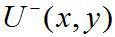
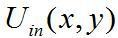
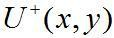
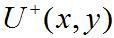
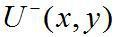
wherein x and y are abscissa and ordinate respectively,![]() are the front wave surface light field distribution data of the target module,
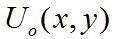
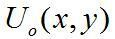
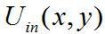
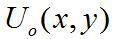
![]() are the light field distribution data of the emitting surface of the light source,
![]() are the Fourier transform function, e is the base of the natural logarithm,
![]() is the imaginary number symbol,
![]() is the wavelength of the emitted light of the light source, is
![]() the distance from the emitting surface of the light source to the front wave surface of the first optical element;
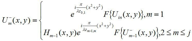
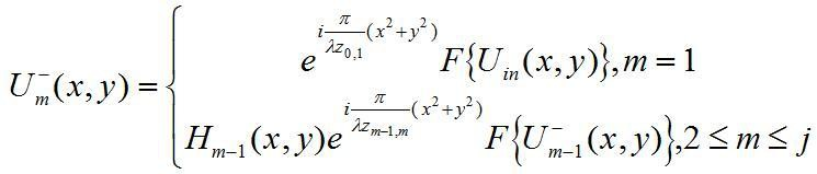
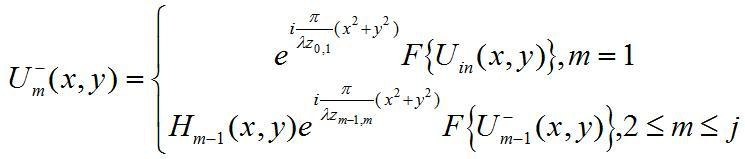
If the forward module comprises an optical element, the front wave surface light field distribution data of the target module is calculated according to the following formula:
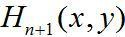
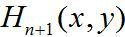
![]() ;
![]() ;
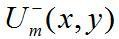
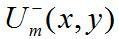
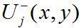
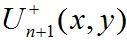
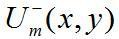
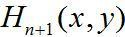
Wherein m is the serial number, is the![]() front wave surface light field distribution data of the m-th optical element,
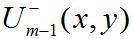
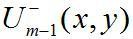
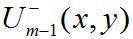
![]() is the front wave-surface light field distribution data of the m-1 optical element,
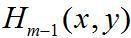
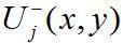
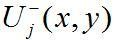
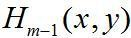
![]() is the transmission function of the m-1 optical element, j is the serial number of the first optical element in the target module, and
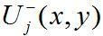
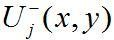
![]() is the front wave-surface light field distribution data
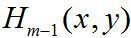
![]() of the j-described optical elementis the distance from the rear wavelength of the m-1 optical element to the front wavelength of the m-1 optical element.
Thus, the front wavesurface light field distribution data of the target module can be obtained through simple calculation.
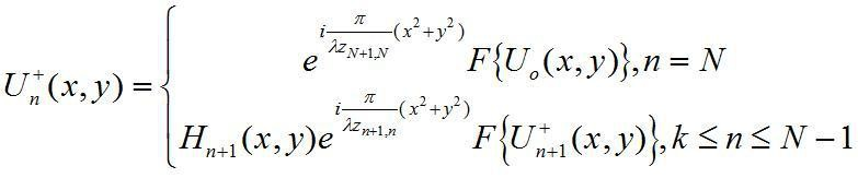
Preferably, Step A3 includes:
If the backward module comprises only the optical sensor, the rear wavesurface light field distribution data of the target module is calculated according to the following formula:
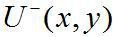
![]() ;
wherein, x and y are abscissa and ordinate respectively,![]() are the light field distribution data of the receiving surface of the optical sensor,
![]() are the Fourier transform function,
![]() are the rear waveplane light field distribution data of the target module, e is the base number of the natural logarithm,
![]() is the imaginary number sign,
![]() is the wavelength of the light emitted by the light source, and N is the total number
![]() of optical elementsis the distance from the receiving surface of the optical sensor to the rear wave surface of the Nth optical element;
If the backward module comprises optical elements, the rear wavesurface light field distribution data of the target module is calculated according to the following formula:
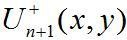
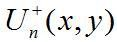
![]() ;
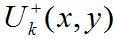
![]() ;
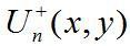
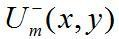
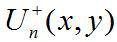
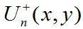
wherein n is the serial number,![]() is the rear waveplane light field distribution data of the nth optical element,
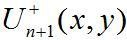
![]() is the rear waveplane light field distribution data of the n+1 optical element,
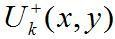
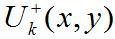
![]() is the transmission function of the n+1st optical element, k is the serial number of the last optical element in the target module,
![]() is the rear wavesurface light field distribution data of the kth optical element,
![]() is n+The distance from the front waveface of the 1st optical element to the rear waveface of the nth optical element.
Thus, the light field distribution data of the rear waveplane of the target module can be obtained through simple calculation.
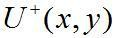
Preferably, in step A4, the metasurface phase distribution data is calculated according to the following formula:
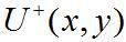
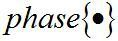
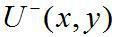
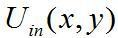
![]() ;
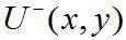
wherein x and y are abscissa and ordinate respectively,![]() are the phase distribution data of the metasurface,
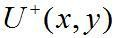
![]() the rear wavesurface light field distribution data of the target module, the
![]() front wavesurface light field distribution data of the target module, and
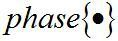
![]() the phase extraction function.
Thus, the phase distribution data of the metasurface can be obtained through simple calculations.
secondly, the application provides a metasurface piece design device for designing a metasurface piece for replacing the target module in the optical system, the optical system comprises a light source, an optical sensor and at least one optical element arranged between the light source and the optical sensor, wherein at least one continuous optical element constitutes the target module, all devices on the front side of the target module form a forward module, and all devices on the rear side of the target module form a backward module;
The metasurface design device comprises:
the acquisition module is used for obtaining the transmission function of each optical element, the light field distribution data of the emitting surface of the light source and the light field distribution data of the receiving surface of the optical sensor;
the first calculation module is used for calculating the front wave surface light field distribution data of the target module according to the transmission function of each optical element and the light field distribution data of the emitting surface of the light source;
the second calculation module is used for calculating the light field distribution data of the rear wave surface of the target module according to the transmission function of each optical element and the light field distribution data of the receiving surface of the optical sensor;
the third calculation module is used for calculating the metasurface phase distribution data according to the front wavesurface light field distribution data of the target module and the rear wave surface light field distribution data of the target module;
The design module is used for designing metasurface members according to the metasurface phase distribution data.
Third, the application provides an electronic device comprising a processor and a memory that stores a computer program that the processor can execute, and when the processor executes the computer program, it runs the steps in the metasurface design method as described above.
Fourth, the application provides a computer-readable storage medium on which a computer program is stored, and when the computer program is executed by a processor, it runs the steps in the metasurface design method as described above.
Fifth, the application provides an optical system optimization method, comprising: obtaining a metasurface piece based on the design method of the metasurface piece described above, and replacing the target module in the original optical system with the metasurface piece.
Preferably, the steps of replacing the target module in the original optical system with the metasurface piece comprise:
if the forward module contains an optical element, the distance between the metasurface of the replaced metasurface piece and the rear waveplane of the last optical element in the forward module is equal to the distance between the rear wavesurface of the last optical element in the forward module in the original optical system and the front waveplane of the first optical element of the target module;
if the forward module comprises only a light source, the distance between the metasurface of the replaced metasurface component and the emitting surface of the light source is equal to the distance between the front wave surface of the first optical element in the original optical system and the emitting surface of the light source;
if the backward module contains an optical element, the distance between the metasurface of the replaced metasurface component and the front waveplane of the first optical element in the backward module is equal to the distance between the front waveplane of the first optical element in the backward module in the original optical system and the rear waveplane of the last optical element of the target module;
If the backward module includes only optical sensors, the distance between the metasurface of the replaced metasurface and the receiving surface of the optical sensor is equal to the distance from the rear wavelength of the last optical element in the original optical system to the receiving surface of the optical sensor.
Beneficial effect: The design method of metasurface parts and related equipment and optical system optimization method provided in the present application only need to obtain the transfer function of each optical element. The light field distribution data of the emitting surface of the light source and the light field distribution data of the receiving surface of the optical sensor can obtain the metasurface phase distribution data of the metasurface piece through simple calculation, and then the metasurface piece is designed according to the metasurface phase distribution data, so that the designed metasurface piece can realize the function of the target module, and after replacing the target module with the metasurface piece, the structure of the optical system can be simplified under the condition that the performance of the optical system remains unchanged.
The specific embodiment
The technical solutions in the embodiments of the present application will be clearly and completely described below in conjunction with the accompanying drawings in the embodiments of the present application, and it is obvious that the described embodiments are only part of the embodiments of the present application, not all embodiments. The components of the embodiment of the present application, which are normally described and shown in the drawings herein, may be arranged and designed in a variety of different configurations. Therefore, the following detailed description of the embodiments of the present application provided in the drawings is not intended to limit the scope of the claimed application, but merely indicates the selected embodiments of the present application. Based on the embodiments of the present application, all other embodiments obtained by a person skilled in the art without creative work fall within the scope of protection of the present application.
It should be noted that similar designations and letters indicate similar terms in the drawings below, so that once an item is defined in a drawing, it does not need to be further defined and explained in subsequent drawings. At the same time, in the description of the present application, the terms "first", "second", etc., are only used to distinguish the description and cannot be construed as indicating or implying relative importance.
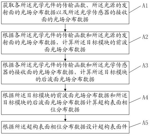
Please refer to FIG. 1, FIG. 1 is a metasurface member design method in some embodiments of the present application, which is used for designing a metasurface member that is used to replace the target module in the optical system, and the optical system comprises a light source, the optical sensor and at least one optical element arranged between the light source and the optical sensor, wherein at least one continuous optical element constitutes a target module (i.e., one of the optical elements forms a target module or therein a plurality of continuous optical elements forms a target module), all devices on the front side of the target module form a forward-facing module, and all devices on the rear side of the target module form a backward-facing module;
The metasurface design method consists of the following steps:
A1. Obtain the transmission function of each optical element, the light field distribution data of the emitting surface of the light source and the light field distribution data of the receiving surface of the optical sensor;
A2. According to the transmission function of each optical element and the light field distribution data of the emission surface of the light source, calculate the front wave surface light field distribution data of the target module;
A3. According to the transmission function of each optical element and the light field distribution data of the receiving surface of the optical sensor, calculate the light field distribution data of the rear waveplane of the target module;
A4. The metasurface phase distribution data is calculated according to the front wavesurface light field distribution data of the target module and the rear wavesurface light field distribution data of the target module;
A5.Design the metasurface parts according to the phase distribution data of the metasurface.
Only need to obtain the transmission function of each optical element, the light field distribution data of the emitting surface of the light source and the light field distribution data of the receiving surface of the optical sensor, the metasurface phase distribution data of the metasurface piece can be obtained through simple calculation, and then the metasurface part is designed according to the metasurface phase distribution data, so that the designed metasurface piece can realize the function of the target module, and after replacing the target module with the metasurface piece, the structure of the optical system can be simplified under the condition that the performance of the optical system remains unchanged.
Wherein, the optical element in the optical system is generally a plurality, but can also be one; the target module is a module composed of the optical element to be replaced in a continuous (refers to sequential continuous), when there is only one optical element, the optical element is the target module, and when there are multiple optical elements, the target module may include one or more optical elements (the sequence of the plurality of optical elements is continuous).
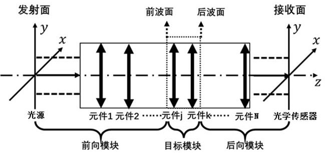
As shown in Figure 4, the optical system (i.e., the original optical system) before optimization comprises a light source, an optical sensor, and N optical elements arranged between the light source and the optical sensor (i.e., element 1 and element 2 in the figure,... , element N), the serial number of each optical element is increased sequentially from the side close to the light source to the side close to the optical sensor, thus, the front side refers to the side close to the light source, the rear side refers to the side close to the optical sensor, the z-axis in the figure coincides with the optical axis of the optical system, the y-axis is facing up, and the direction of the x-axis is determined by the right-hand rule, wherein, the light source and the front j-1 optical element form a forward module, and the j-th optical element forms the target module to the k-th optical element (i.e., the serial number of the first optical element in the j-target module, and the serial number of the last optical element in the target module when k) , the k+1st optical element to the Nth optical element and the optical sensor form the backward module.
Among them, optical components include, but are not limited to, lenses, mirrors, and other devices that use thickness and/or surface to change beam characteristics to control beam transmission.
Among them, one optical element can be used as the target module, and the combination of any continuous multiple optical components can be used as the target module. For example, in Figure 4, j can be equal to 1, k can be equal to N, when j = 1, the light source is a forward module, when k = N, the optical sensor is a backward module, and when j = 1 and k = N, the target module consists of all optical elements. Generally, k is greater than j, but it can also be equal to j, and when k is equal to j, it means that the target module includes only one optical element (generally, when an optical element has a complex structure, large footprint and/or high price, it can be replaced with a metasurface piece).
Among them, the light field distribution data in the present application refers to the distribution data of light intensity. In step A1, the light field distribution data of the emitting surface of the light source is the distribution data of the light intensity on the emitting surface, and the light field distribution data of the receiving surface of the optical sensor is the distribution data of the light intensity on the receiving surface. The light field distribution data of the emitting surface of the light source and the light field distribution data of the receiving surface of the optical sensor can be measured in advance.
Wherein, in step A1, the transfer function of the optical element can be calculated according to the characteristics of the element and the principle of diffraction calculation, or the transfer function of the optical element can be obtained through simulation calculation. In general, for optical elements with simple structure, the transfer function can be calculated according to the element characteristics and diffraction calculation principle of the optical element (the specific calculation method is the prior art, which is not described in detail here), and for the optical element with complex structure, the transfer function can be obtained by simulation calculation (for example, simulation calculation by finite element method or finite difference time domain method).
Specifically, Step A2 includes:
If the forward module includes only light sources (i.e., j=1), the front-waveplane light field distribution data of the target module is calculated according to the following formula:
![]() ;
wherein, x and y are abscissa and ordinate respectively (as shown in Figure 4, the z-axis of the right-hand coordinate system xyz coincides with the optical axis of the optical system, and the positive z-axis direction is from front to back, the x-axis and y-axis are perpendicular to the z-axis, and the x-axis and y-axis are perpendicular to each other, the abscissa is the x-axis coordinates, and the ordinate is the y-axis coordinates),![]() the front wave surface light field distribution data of the target module,
![]() the light field distribution data of the emission surface of the light source,
![]() the Fourier transform function, and e is the base of the natural logarithm,
![]() is the imaginary symbol,
![]() which is the wavelength of the emitted light of the light source, and
![]() the distance from the emitting surface of the light source to the front wave surface of the first optical element (is a known value);
If the forward module contains optical components (i.e., j≥2), the front-wavelength field distribution data of the target module is calculated according to the following formula:
![]() ;
![]() ;
wherein m is the serial number, which is the![]() front waveplane light field distribution data of the m-th optical element,
![]() the front-wave surface light field distribution data of the m-1 optical element,
![]() the transmission function of the m-1 optical element, and the serial number of the first optical element in the target module, and
![]() the front wavefront light field distribution data
![]() of the j-th optical elementis the distance from the rear wavesurface of the m-1 optical element to the front wavesurface of the m-1 optical element (both are known values), specifically, according to the above formula, in the order of m=1 to m=j (i.e., the ascending order of m), it is calculated
![]() in order until it is calculated, and the front wavesurface light field distribution data that is used as the
![]() target module is calculated
![]() .
Thus, the front wavesurface light field distribution data of the target module can be obtained through simple calculation.
Specifically, Step A3 includes:
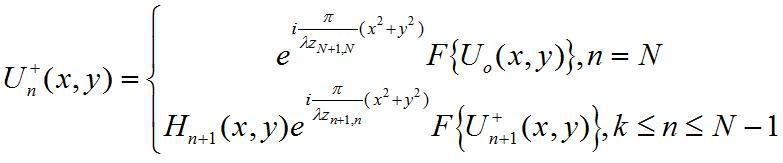
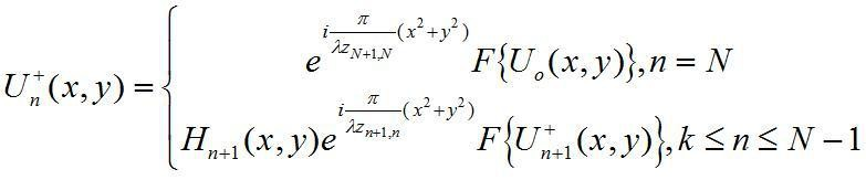
If the backward module includes only optical sensors (i.e., k=N), the back-waveplane light field distribution data of the target module is calculated according to the following formula:
![]() ;
wherein![]() is the light field distribution data of the receiving surface of the optical sensor,
![]() which is the Fourier transform function, the
![]() light field distribution data of the rear waveplane of the target module, and
![]() the distance from the receiving surface of the optical sensor to the rear wavelength of the Nth optical element (is a known value);
If the backward module contains optics (i.e., k≤N-1), the back-waveplane light field distribution data of the target module is calculated according to the following formula:
![]() ;
![]() ;
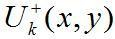
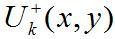
wherein n is the serial number,![]() which is the rear waveplane light field distribution data of the nth optical element,
![]() the rear waveplane light field distribution data of the n+1st optical element,
![]() and the transfer function of the n+1st optical element, and k is the serial number of the last optical element in the target module, and
![]() the rear wavesurface light field distribution data of the kth optical element,
![]() which is the n+Specifically, according to the above formula, the distance from the front waveplane of one optical element to the rear waveplane of the nth optical element (both are known values), and in the order of n=N to n=k (i.e., the descending order of n), it is calculated
![]() in order until it is calculated
![]() , and the
![]() light field distribution data of the rear waveplane as the target module is calculated.
Thus, the light field distribution data of the rear waveplane of the target module can be obtained through simple calculation.
Specifically, in step A4, the metasurface phase distribution data is calculated according to the following formula:
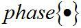
![]() ;
Among them, the![]() phase distribution data of the metasurface is the
![]() phase extraction function.
Thus, the phase distribution data of the metasurface can be obtained through simple calculations.
Wherein, in step A5, the design of the metasurface piece according to the metasurface phase distribution data is specifically to design the micro-nano structure on the metasurface of the metasurface according to the metasurface phase distribution data, and the specific design method is the prior art, which is not described in detail here.
From the above, it can be seen that the metasurface design method obtains the transfer function of each optical element, The light field distribution data of the emitting surface of the light source and the receiving surface of the optical sensor; the light field distribution data of the front wave plane of the target module are calculated according to the transmission function of each optical element and the light field distribution data of the emission surface of the light source; the light field distribution data of the rear wave surface of the target module is calculated according to the transmission function of each optical element and the light field distribution data of the receiving surface of the optical sensor; the phase distribution data of the metasurface is calculated according to the front wave surface light field distribution data of the target module and the rear wave surface light field distribution data of the target module; and the metasurface parts are designed according to the phase distribution data of the metasurfaceTherefore, the designed metasurface parts can realize the functions jointly realized by the combination of replaced optical components, which is conducive to simplifying the structure of the optical system.
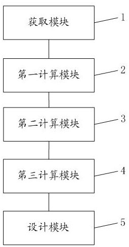
Referring to Fig. 2, the application provides a metasurface device design device for designing a metasurface piece for replacing the target module in the optical system, the optical system comprises a light source, an optical sensor and at least one optical element arranged between the light source and the optical sensor, wherein at least one continuous optical element constitutes a target module, all devices on the front side of the target module form a forward module, and all devices on the rear side of the target module form a backward module;
The metasurface design device comprises:
obtain module 1, which is used for obtaining the transfer function of each optical element, the light field distribution data of the emitting surface of the light source and the light field distribution data of the receiving surface of the optical sensor (refer specifically to step A1 of the preceding article);
the first calculation module 2 is used for calculating the front wave surface light field distribution data of the target module according to the transmission function of each optical element and the light field distribution data of the emission surface of the light source (specifically refer to step A2 of the preceding article);
the second calculation module 3 is used for calculating the light field distribution data of the rear wavelength surface of the target module according to the transmission function of each optical element and the light field distribution data of the receiving surface of the optical sensor (specifically refer to step A3 of the preceding article);
the third calculation module 4 is used for calculating the metasurface phase distribution data according to the front wave surface light field distribution data of the target module and the rear wave surface light field distribution data of the target module (specifically refer to step A4 of the preceding article);
The design module 5 is used to design the metasurface piece based on the metasurface phase distribution data (refer to step A5 above).
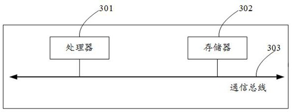
Please refer to FIG. 3, FIG. 3 is a schematic diagram of the structure of an electronic device provided for the embodiment of the present application, and the present application provides an electronic device comprising: a processor 301 and a memory 302, a processor 301 and a memory 302 through a communication bus 303 and/ or other forms of connecting mechanisms (not indicated) are interconnected and communicate with each other, the memory 302 stores an executable computer program of the processor 301, and when the electronic device is running, the processor 301 executes the computer program to perform a metasurface piece design method in any of the optional embodiments of the above embodiment, so as to realize the following functions: obtaining the transfer function of each optical element, The light field distribution data of the emitting surface of the light source and the receiving surface of the optical sensor; the light field distribution data of the front wave plane of the target module are calculated according to the transmission function of each optical element and the light field distribution data of the emission surface of the light source; the light field distribution data of the rear wave surface of the target module is calculated according to the transmission function of each optical element and the light field distribution data of the receiving surface of the optical sensor; the phase distribution data of the metasurface is calculated according to the front wave surface light field distribution data of the target module and the rear wave surface light field distribution data of the target module; and the metasurface parts are designed according to the phase distribution data of the metasurface。
The embodiment of the present application provides a computer-readable storage medium, on which a computer program is stored, and when the computer program is executed by a processor, a metasurface piece design method in any of the optional embodiments of the above embodiment is executed to realize the following functions: obtaining the transfer function of each optical element, The light field distribution data of the emitting surface of the light source and the receiving surface of the optical sensor; the light field distribution data of the front wave plane of the target module are calculated according to the transmission function of each optical element and the light field distribution data of the emission surface of the light source; the light field distribution data of the rear wave surface of the target module is calculated according to the transmission function of each optical element and the light field distribution data of the receiving surface of the optical sensor; the phase distribution data of the metasurface is calculated according to the front wave surface light field distribution data of the target module and the rear wave surface light field distribution data of the target module; and the metasurface parts are designed according to the phase distribution data of the metasurface。 Among them, computer-readable storage media can be implemented by any type of volatile or non-volatile storage device or a combination thereof, such as Static Random Access Memory (SRAM), Electrically Erasable ProgrammableRead-Only Memory, EEPROM), Erasable ProgrammableRead Only Memory (EPROM), Programmable Red-Only Memory (PROM), Read-Only Memory (ROM), magnetic memory, flash memory, disks or optical discs.
The application also provides an optical system optimization method, comprising: obtaining a metasurface component based on the design method of the metasurface element described above, and replacing the target module in the original optical system with the metasurface component.
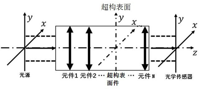
For example, Figure 4 is the original optical system, and Figure 5 is the optimized optical system, which simplifies the structure of the optical system while keeping the performance of the optical system unchanged by replacing the original j-k-k optical element with a metasurface piece.
Preferably, the steps to replace the target module in the original optical system with a metasurface include:
if the forward module comprises an optical element (i.e., j≥2), the distance between the metasurface of the replaced metasurface component and the rear wavesurface of the last optical element in the forward module is equal to the distance between the rear wavesurface of the last optical element in the forward module in the original optical system and the front wavelength of the first optical element of the target module;
if the forward module only includes a light source (i.e., j=1), the distance between the metasurface of the replaced metasurface and the emitting surface of the light source is equal to the distance between the front wave surface of the first optical element in the original optical system and the emitting surface of the light source;
if the backward module comprises an optical element (i.e., k≤N-1), the distance between the metasurface of the replaced metasurface and the front wavesurface of the first optical element in the backward module is equal to the distance between the front waveplane of the first optical element in the backward module in the original optical system and the rear waveplane of the last optical element of the target module;
If the backward module includes only an optical sensor (i.e., k=N), the distance between the metasurface of the replaced metasurface and the receiving surface of the optical sensor is equal to the distance from the rear wavelength of the last optical element in the original optical system to the receiving surface of the optical sensor.
This ensures that the performance of the replaced optical system remains the same as that of the original optical system.
In the embodiments provided in the present application, it should be understood that the disclosed apparatus and method may be realized by other means. The device embodiments described above are only schematic, for example, the division of the units is only a logical function division, and there may be another division mode when the actual implementation is realized, and for example, a plurality of units or components can be combined or can be integrated into another system, or some features can be ignored, or not executed. On the other hand, the coupling or direct coupling or communication connection between each other shown or discussed may be indirect coupling or communication connection through some communication interface, device or unit, which may be in electrical, mechanical or other form.
In addition, the cells described as detached parts may or may not be physically separated, and the parts shown as units may or may not be physical units, located in one place, or distributed across multiple network units. Some or all of these units can be selected according to actual needs to realize the purpose of the present embodiment.
Furthermore, each functional module in each embodiment of the present application may be integrated together to form an independent part, or each module may exist independently, or two or more modules may be integrated to form an independent part.
For the purposes of this article, relational terms such as first and second, etc., are used solely to distinguish one entity or operation from another, and do not necessarily require or imply any such actual relationship or sequence between those entities or operations.
The foregoing is only an embodiment of the present application and is not intended to limit the scope of protection of the present application, which is subject to various changes and variations for those skilled in the art. Any amendments, equivalent replacements, improvements, etc., made within the spirit and principles of this application shall be included in the scope of protection of this application.
















































 400-4929-0909
 contact@catarc.com.cn