Contents of the invention
The main object of the present invention is to provide a photodetector, aiming to solve the technical problem that the light is repeatedly reflected between the bottom connecting layer and the silicon base layer in the prior art, resulting in the reduction of the light absorption efficiency of the silicon base layer.
In order to achieve the above purpose, the invention proposes a photodetector, and the photodetector comprises:
silicon base layer, the two opposite sides on the silicon base layer are respectively the light entering surface and the light exiting surface;
the connecting layer is arranged on the glossy surface;
the first light trap layer is arranged on one side of the light entry surface facing the light exit surface;
the second light trapping layer is arranged on one side of the light outlet surface facing the light entry surface;
the grating layer is arranged between the connecting layer and the grating surface.
optionally, the glossing surface is provided with a first electrode area, a first installation area enclosed in the first electrode area, and a second electrode area enclosed around the first installation area;
the second light trapping layer comprises a plurality of second projections, the second projections are uniformly spaced at intervals in the first installation area, and the first electrode area and the second electrode area are used for connecting external electrodes.
Optionally, the interval between any two adjacent second bumps is 50nm~200nm.
Optionally, the second bump is in the form of a quadrangular pyramid, the projection of the second bump in the direction of the perpendicular gloss surface is in a positive direction, and the side length of the square projection of the second bump is 600nm~800nm.
Optionally, the grating layer comprises a plurality of grating strips, and the grating bars are arranged at intervals between the connecting layer and the grating surface;
Wherein, a plurality of second bumps are distributed in an array, and the grating bars are parallel to the row direction or column direction of the array.
optionally, a second installation area is provided on one side of the connecting layer facing the glossy surface, and the position of the second installation area corresponds to the position of the first installation area;
a plurality of grating strips are arranged at intervals in the second installation area.
Optionally, the thickness of the grating strip is 100nm~300nm, the width is 100nm~300nm, and the spacing between any two adjacent grating strips is 50nm~200nm.
Optionally, the first light trapping layer comprises a plurality of first bumps, and the plurality of first bumps are uniformly spaced on the light entering surface.
Optionally, the photodetector further comprises a reflector, the reflector is arranged in the connecting layer, and the position of the reflector corresponds to the position of the grating layer.
Optionally, the photodetector further comprises an isolation layer, and the isolation layer is arranged on the side wall of the silicon base layer.
The technical scheme of the present invention is respectively provided with a light trap layer on the light entering surface and the light outlet surface of the silicon base layer, under the effect of the second light trapping layer, the surface structure of the light outlet surface has been changed, the reflectivity of light entering the light outlet surface has been reduced, and the plasmon polaron effect is formed with the grating layer and the silicon, and the light absorption efficiency of the silicon base layer is enhanced. Under the action of the first light trap layer, the reflectivity of the light is improved, the light is prevented from being emitted from the light entering surface, and the light absorption rate of the silicon base layer is greatly improved.
The specific embodiment
The technical solutions in the embodiments of the present invention will be clearly and completely described below in conjunction with the accompanying drawings in the embodiments of the present invention, and it is obvious that the described embodiments are only part of the embodiments of the present invention, not all embodiments. Based on the embodiments in the present invention, all other embodiments obtained by a person skilled in the art without making creative labor belong to the scope of protection of the present invention.
It should be noted that all directional indications in the embodiments of the present invention (such as up, down, left, right, front, rear...... ) is only used to explain the relative position relationship between the parts under a specific attitude (as shown in the attached drawing), the movement, etc., and if the specific attitude changes, the directional indication will change accordingly.
In addition, descriptions such as "first", "second", etc., in the present invention are for descriptive purposes only and cannot be construed as indicating or implying their relative importance or implying the number of technical features indicated. Thus, defining the "first" and "second" features may explicitly or implicitly include at least one of those features. In the description of the present invention, "plurality" means at least two, such as two, three, etc., unless otherwise expressly and specifically qualified.
In the present invention, unless otherwise expressly specified and qualified, the terms "connection", "fixed", etc., shall be construed broadly, for example, "fixed" may be a fixed connection, a detachable connection, or a whole, a mechanical connection, an electrical connection, a direct connection, or an indirect connection through an intermediate medium, or an internal connection of two elements or an interaction between two elements, unless otherwise expressly defined. For a person of ordinary skill in the art, the specific meaning of the above terms in the present invention may be understood according to the specific circumstances.
In addition, the technical solutions between the various embodiments of the present invention may be combined with each other, but must be based on those capable of being realized by a person skilled in the art, and when the combination of technical solutions contradicts each other or cannot be realized, it shall be considered that the combination of such technical solutions does not exist, and is not within the scope of protection claimed by the present invention.
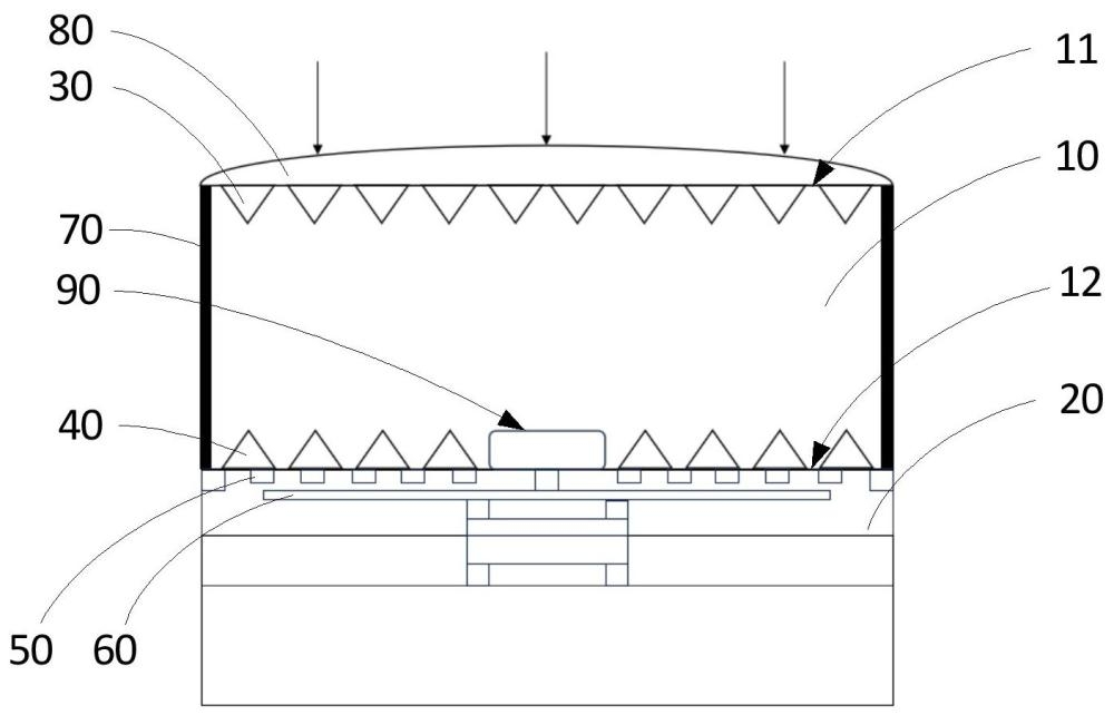
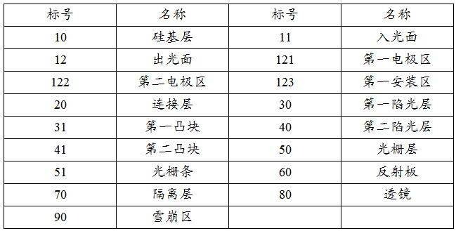
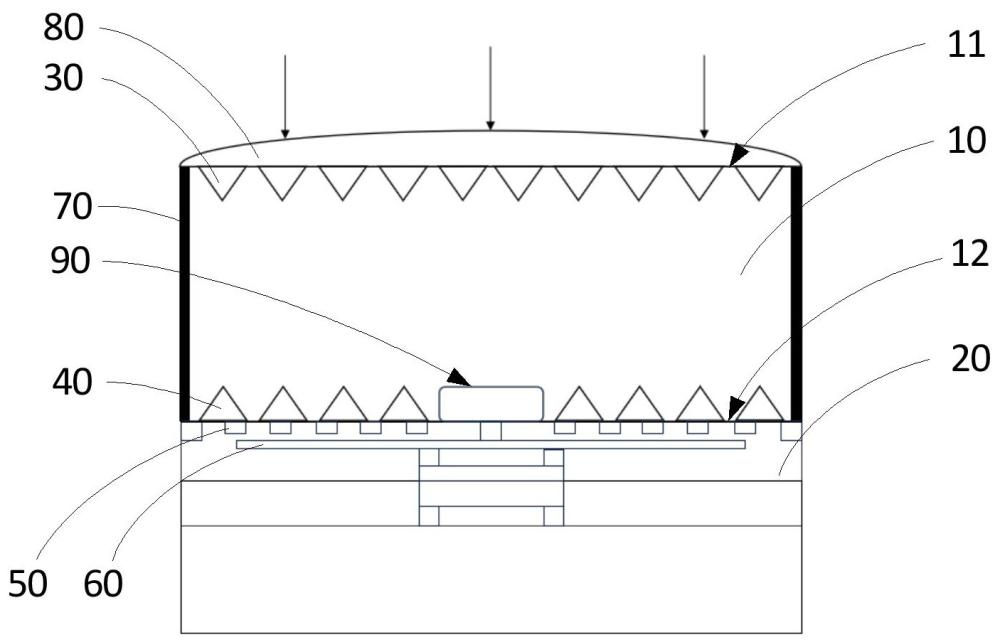
The invention provides a photodetector, and the photodetector comprises a silicon base 10, a connecting layer 20, a first light trapping layer 30, the second light trapping layer 40 and the grating layer 50, the two opposite sides of the silicon base layer 10 are respectively the light entering surface 11 and the light outlet surface 12; the connecting layer 20 is arranged on the light outlet surface 12; the first light trapping layer 30 is arranged on one side of the light entering surface 11 towards the light outlet surface 12; the second light trapping layer 40 is arranged on one side of the light outlet surface 12 towards the light entering surface 11; and the grating layer 50 is arranged between the connecting layer 20 and the light outlet surface 12.
In this embodiment, the silicon base layer 10 adopts a back-side illumination (BSI) avalanche diode (Single Photon Avalanche Diode, SPAD) structure to inject ions into the silicon base layer 10, and the connecting layer 20 is used for installing a circuit for installing the SPAD and the electrical connection of the external power supply or equipment. The back-illuminated process directly flips the SPAD of the electrode and the lead wire and connects it with the circuit in the connection layer 20 below, and then thins the upper part of the SPAD to the target thickness, thereby greatly increasing the fill factor of the SPAD and improving the photoelectric detection efficiency.
Please refer to Fig. 1, the incident light enters the silicon base layer 10 from the light entering surface 11, and through the silicon base layer 10 it is emitted from the light surface 12 at the bottom, and part of the light is reflected and enters the silicon base layer 10 again under the effect of the connecting layer 20.
the silicon base layer 10 has an avalanche zone 90, and the light path of the incident light can also be increased by adjusting the size of the avalanche zone 90 in the silicon base layer 10, and the incident light is usually near-infrared light. The incident light is absorbed in the silicon base layer 10 and initiates an avalanche in the migration to the avalanche zone 90. The incident light that is not absorbed is emitted from the luminous surface 12 and is finally reflected back to the silicon base layer 10 by the connecting layer 20.
A wafer layer may also be arranged at the bottom of the connecting layer 20, that is, on one side where the connecting layer 20 deviates from the silicon base layer 10. the connecting layer 20 is made of silicon dioxide, and a metal connection is formed on the connecting layer 20 by etching, embedding, etc. and bonding to the wafer body in the bottom wafer layer. Near-infrared light passes through the silicon base layer 10, and the detected electrical signal is sent to the wafer layer through the line.
Among them, the absorption of near-infrared light by silica is 0. In addition, the connecting layer 20 can also be prepared by adopting other materials with the same or similar properties.
In order to improve the absorption efficiency of near-infrared light, a first light trap layer 30 is arranged on the inner side of the light entering surface 11, that is, on one side towards the light exit surface 12, and at the same time, a second light trapping layer 40 is arranged on the inner side of the light entering surface 12, that is, on one side facing the light entering surface 11. After setting the sinkhole, the sinkhole layer needs to be flattened.
A lens 80 can also be installed on the outer side of the light-entering surface 11, and the lens 80 may adopt a convex lens 80, so that the effect of light convergence is played, so that more near-infrared light passes through the light-entering surface 11 and enters the silicon base layer 10.
When near-infrared light enters the silicon base layer 10 through the light-entering surface 11, part of the near-infrared light will be reflected to the light-entering surface 11 due to the reflection effect, therefore, under the action of the first light-trapping layer 30, the near-infrared light is reflected again through the surface of the first light-trapping layer 30, so as to avoid it from emitting out of the light-entering surface 11, so as to play the role of near-infrared light being limited in the silicon base layer 10, so as to improve the light absorption rate of the silicon base layer 10.
In addition, by adjusting the surface shape of the first light trap layer 30, the near-infrared light can produce a diffuse reflection effect, and the optical path of the near-infrared light in the silicon base layer 10 is further increased, so that the absorption rate of the near-infrared light is improved.
As an embodiment, the effect of changing the surface shape is achieved by arranging a plurality of bumps on the glossy surface 11 to form the first light-trapping layer 30. Specifically, the first light trapping layer 30 comprises a plurality of first projections 31, and a plurality of first projections 31 are uniformly spaced on the light entering surface 11.
The first bump 31 can adopt a quadrangular pyramid structure, please refer to Figure 1, and the cross-section of the first bump 31 is triangular. a plurality of first bumps 31 are arranged at intervals to form a zigzag structure, and after near-infrared light is injected, the diffuse reflection effect of the first light trap layer 30 is realized in the first light trap layer 30.
When near-infrared light passes through the silicon base layer 10, it will eventually be emitted to the luminous surface 12. In the same way, a plurality of second projections 41 are arranged on the glossy surface 12 to form the second light-trapping layer 40. The shape of the second bump 41 is similar to that of the first bump 31. Similarly, to prevent near-infrared light from being emitted from the silicon base layer 10, under the mutual cooperation of the first light trap layer 30 and the second light trap layer 40, the effect of near-infrared light "locking" in the silicon base layer 10 is realized, and the light absorption rate of the silicon base layer 10 is improved.
However, it should be noted that, in order to electrically connect the connecting layer 20 with the wafer at the bottom, an electrode needs to be arranged on one side of the glossy surface 12.
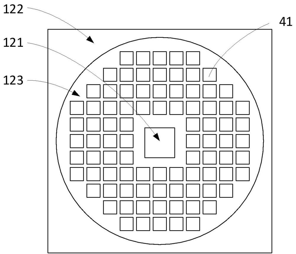
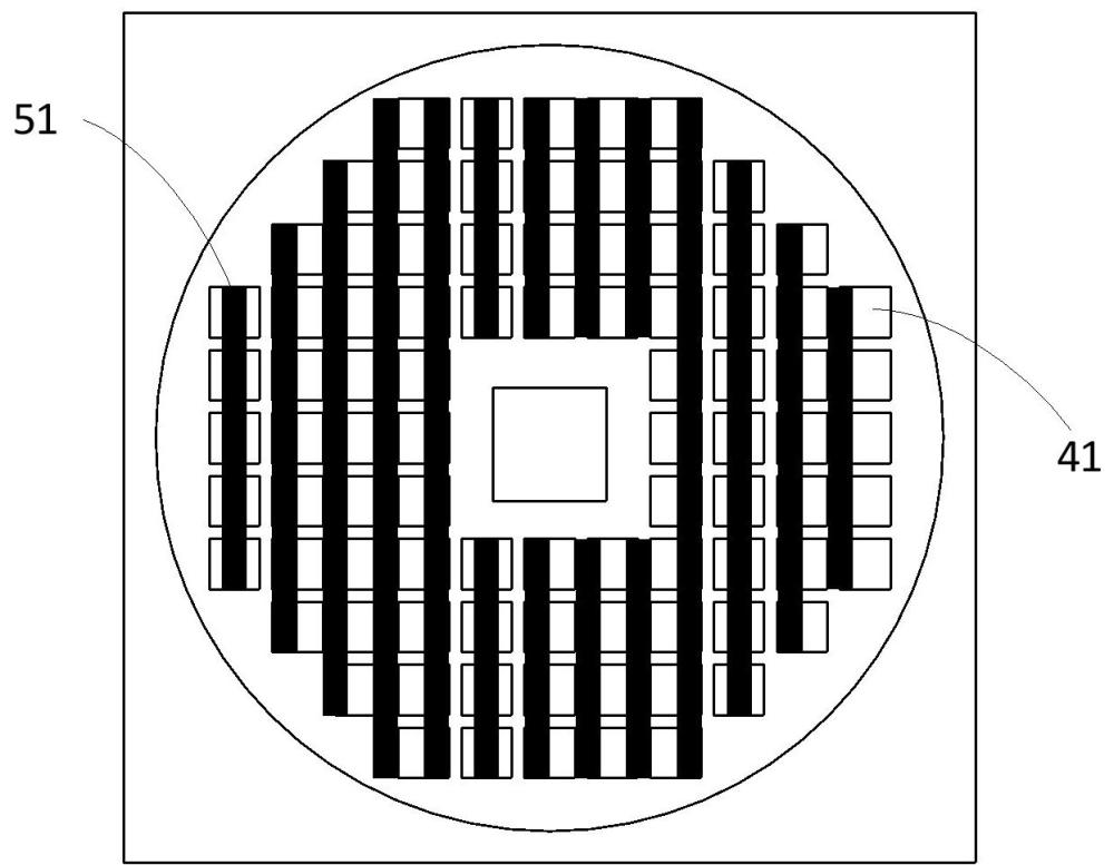
Therefore, with reference to Fig. 2, the glossy surface 12 has a first electrode area 121, a first installation area 123 enclosed in the first electrode area 121, and a second electrode area 122 enclosed around the first installation area 123.
In this embodiment, a charge focusing (charge focusing) structure is used, and the first electrode region 121 and the second electrode region 122 for connecting with the electrode need to be reserved on one side of the glossy surface 12.
the first electrode area 121 may be arranged at the central position of the glossy surface 12, the first installation area 123 is wrapped in an annular shape around the first electrode area 121, and the remaining edge portion on the glossy surface 12 is finally used as the second electrode area 122.
Wherein, the first electrode area 121 is electrically connected with the SPAD cathode, the second electrode area 122 is electrically connected with the SPAD anode, and the first installation area 123 arranged in the middle in a ring shape is used for installing a plurality of second projections 41.
In the scheme, when detecting near-infrared light in different directions, the installation direction of the light entering surface 11 can be adjusted, such as to the left or to the right.
At the same time, under the effect of the grating layer 50, the grating layer 50 and the second light trap layer 40 cooperate with each other, so that the near-infrared light can produce a diffraction effect and change its light field distribution. At the same time, the plasma miciton effect is also produced between the grating layer 50 and the silicon base layer 10, and the infrared absorption rate of the silicon base layer 10 is increased.
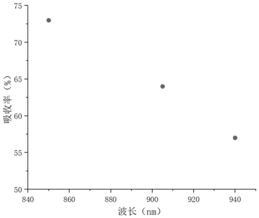
In this embodiment, through the FDTD light field simulation, please refer to Figure 4, when the wavelength of near-infrared light is about 850 nm, the light absorption rate is 73%, when the wavelength of near-infrared light is about 905 nm, the light absorption rate is 64%, and when the wavelength of near-infrared light is about 940 nm, the light absorption rate is 57%. It is concluded that the light absorption rate of near-infrared light in all wavelength bands is significantly improved.
The technical scheme of the present invention is respectively provided with a light trap layer on the light entering surface 11 and the light outlet surface 12 of the silicon base layer 10, under the effect of the second light trapping layer 40, the surface structure of the light outlet surface 12 has been changed, the reflectivity of the light when entering the light outlet surface 12 has been reduced, and the grating layer 50 forms a plasmonic polarion effect with the silicon, and the light absorption efficiency of the silicon base layer 10 has been enhanced. Under the effect of the first light trap layer 30, the reflectivity of light is improved, the light is prevented from being emitted from the light entering surface 11, and the light absorption rate of the silicon base layer 10 is greatly improved.
Further, the grating layer 50 comprises a plurality of grating strips 51, and the grating strips 51 are arranged at intervals between the connecting layer 20 and the grating surface 12;
In order to ensure that the grating strip 51 can form a plasmon effect with the silicon base layer 10, and enhance the light absorption rate of the silicon base layer 10. The position of the grating strip 51 should correspond to the position of the second projection 41. Therefore, a ring-shaped second installation area is similarly arranged on one side of the connecting layer 20 toward the glossy surface 12, and the first installation area 123 overlaps with the projection of the second installation area in the direction of the perpendicular glossing surface 12.
In this embodiment, the arrays between the plurality of the second bumps 41 are distributed in the first installation area 123, and when installed, the grating strips 51 are kept parallel to the row or column directions of the second bumps 41 arrays, and the dimensions of the second bumps 41 and the grating bars 51 can be controlled and adjusted so that each grating bar 51 can cover a row or a column of the second bumps 41.
Please refer to Fig. 2, the second projection 41 is a quadrangular pyramid, the projection of the second projection 41 in the direction of the perpendicular surface 12 is in a positive direction, and the grating strip 51 is a quadrilateral in the shape of a long strip. The side length of the square projection of the second bump 41 is 600nm~800nm, and the interval between any two adjacent second bumps 41 is 50nm~200nm. Please refer to Figure 3, the width of the grating strip 51 is 100nm~300nm, and the spacing between any two adjacent grating strips 51 is 50nm~200nm. By adjusting the dimensions of the second bumper 41 and the grating bar 51, ensure that the grating bar 51 can cover the second bumper 41 in each row or column.
Further, the photodetector further comprises a reflector 60, the reflector 60 is arranged in the connecting layer 20, and the position of the reflector 60 corresponds to the position of the grating layer 50. After passing through the silicon base layer 10, near-infrared light is finally emitted from the glossing surface 12.
the reflector 60 is close to one side of the connecting layer 20 close to the silicon base 10, and is made of metal material, so that after the near-infrared light is emitted from the luminous surface 12, it is emitted into the reflector 60, and under the effect of the reflector 60, the near-infrared light is reflected and enters into the silicon base 10 again from the luminous surface 12, and is reabsorbed by the silicon base 10. Further improve the absorption efficiency of the overall near-infrared light and improve the detection accuracy.
Further, the photodetector further comprises an isolation layer 70, and the isolation layer 70 is arranged on the side wall of the silicon base layer 10.
the isolation layer 70 is arranged on the inner side of the side wall of the silicon base layer 10, wherein the side wall of the silicon base layer 10 refers to the connecting wall connecting the glossy surface 12 and the glossy surface 11. Please refer to Figure 1, the side wall is perpendicular to the light surface 12 and the light surface 11, and the shape or size of the side wall can be adjusted according to the requirements of different experiments for optical properties.
The isolation layer 70 wraps the side wall of the entire silicon base layer 10 for optical crosstalk isolation. In addition, under the effect of the isolation layer 70, it can also prevent the high voltage from penetrating the wrapped silicon base layer 10. Improves overall stability.
The above is only a preferred embodiment of the present invention, and does not limit the patent scope of the present invention, and all equivalent structural transformations made by using the contents of the description and drawings of the present invention under the invention conception, or directly or indirectly used in other related technical fields are included in the patent protection scope of the present invention.










 400-4929-0909
 contact@catarc.com.cn